This particular chip was a free sample from Maxim Integrated (thanks, guys!) direct from their factory/distribution system and so is guaranteed to be authentic. Unlike my previous attempt (which involved physically grinding the package down and delicately picking out the silicon die and crystal), this chip I dissolved in hot nitric acid in a fume hood for about 30-45 minutes. I then washed it with deionized water followed by an isopropanol rinse. Unfortunately, this process left the die either with some sort of residue, or incompletely etched certain parts, so there’s what looks to be “water marks” around the chip (this is distinctly noticeable in the large block in the top-left).
The image is a composite. To make it, I first focus-stacked (using PICOLAY) a dozen or so images that cover the same, small area of the chip with different depths of field in each photo. I then moved the field of view to a neighboring region of the chip and repeated the process. The focus-stacked images were then stitched using the Microsoft Image Composite Editor resulting in a single large, high-resolution image whereby everything is (I hope) in focus.
Unsurprisingly, the die layout is completely different from that of the DS3231, presumably due to the differences in driving and collecting signals from a crystal oscillator and a MEMS oscillator. The crystal-based DS3231 switches in or out tiny on-die capacitors to slightly change the frequency of the oscillator to compensate for variations in temperature while the DS3231M uses “digital adjustment controller logic” to adjust the final 1 Hz output that one can access on the SQW pin and which also is fed into the internal clock circuitry.
I’m uncertain if the MEMS oscillator is supposed to be on the die (if so, I didn’t see it — perhaps readers might have better luck) or in the package itself (though I didn’t see it when I picked the die out of the acid, but there was a lot of gunk from the dissolved package).
What’s the deal with the enormous metal section in the lower-middle-left? I haven’t the foggiest.
Any thoughts or ideas? If you have any insight I’d love to hear it.
A while back I needed to interface a GPS timing receiver that only has an RS-232 serial connection with one of my Raspberry Pis. The Pi only supports TTL-level serial and only tolerates voltages between 0-3.3V its the UART pins.
Enter the MAX3232, a chip from Maxim Integrated that converts between RS-232 and TTL serial with supply voltages from 3.0 to 5.5V. It produces “true” RS-232-level voltages (both positive and negative) using built-in charge pumps and some small external capacitors. Just the ticket for what I needed.
Alas, the MAX3232 isn’t really something one can run down to the local electronics shop (and there isn’t any such shop where I live in Switzerland, as far as I know) and pick up. Typically it’s purchased by manufacturers in quantity from major suppliers. Hobbyists like myself need to turn to the internet where such things are available in abundance for cheap from China, though one must be wary of counterfeits. Of course, I could order from legitimate Swiss distributors, but small-quantity pricing and shipping are extremely high (>$10 USD per chip!) compared to major US distributors like DigiKey and Mouser.
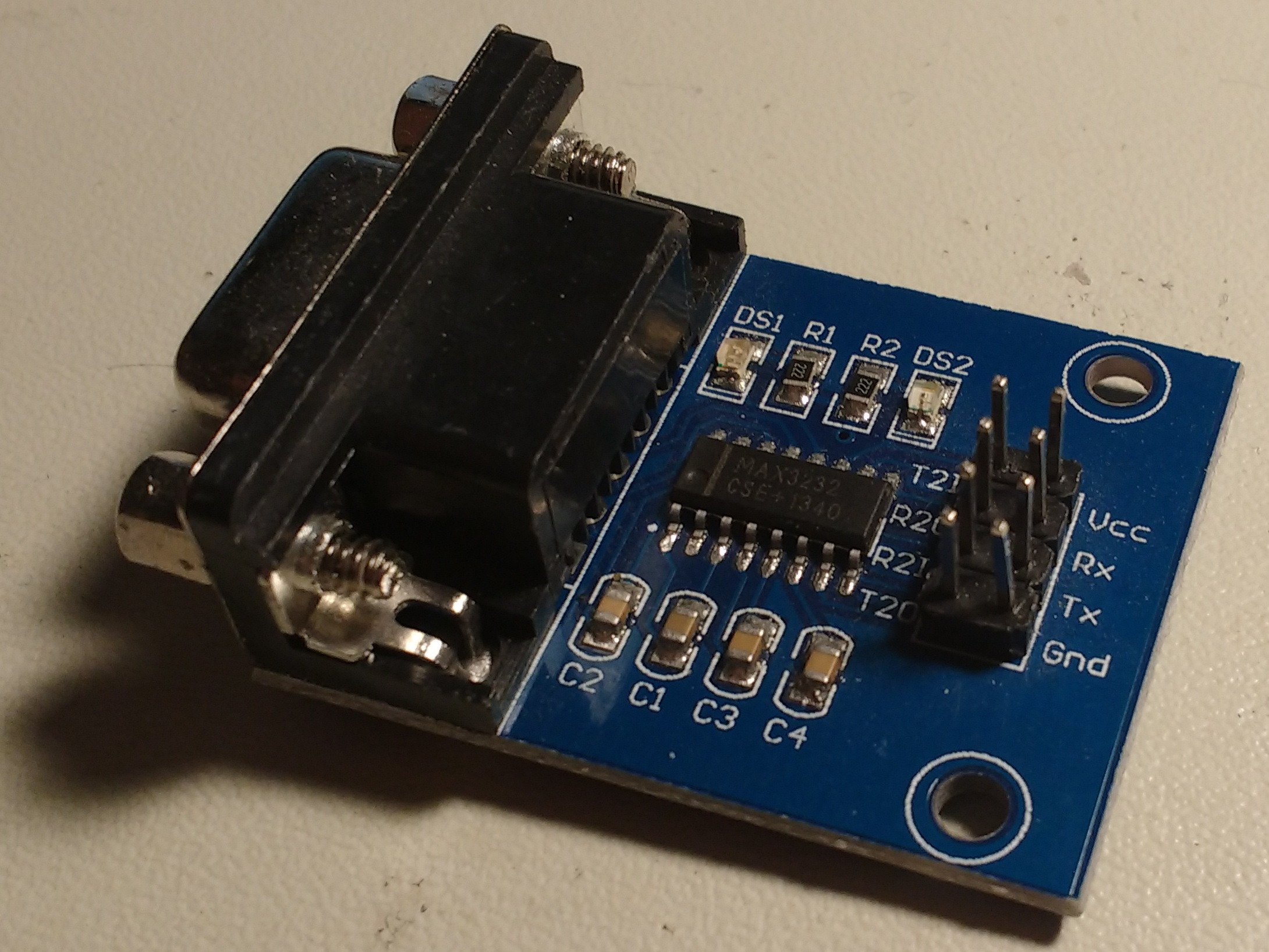
In my case, I ended up buying a few boards like this one from an online vendor in China. The listing specifically states it had a MAX3232 chip. My thought was that if it was a legitimate chip, cool. If not, it’d be an interesting experiment and I’d get some cheap DE-9 connectors out of the deal.
Fake “MAX3232” Board
To the naked eye, everything seemed to be reasonable. The chip did have markings identifying it as a MAX3232 (falsely, as I later discovered; read on!). The board worked and the chip functioned within the specs in the Maxim datasheet and it even broke out the chip’s second RS-232-to-TTL channel on the header pins.
However, the first board failed after a few weeks, drew significant current, and dramatically overheated. By “overheated” I mean “blister-raising burn on my fingertip”-level-hot. Also, the data-transfer LEDs were glowing faintly all the time rather than flickering on and off when data was flowing.
Figuring this was just some bad luck on my part (this is before I got the anti-static mat on my desk), I swapped it out for another board. I was particularly careful with anti-static precautions, and put the board over a small glass container just in case it overheated and caught fire. Although it didn’t catch fire (thankfully!), it did fail after a few weeks and overheated just like the first one.
Ok, so something’s going on, but what? Since the chips had obviously failed, I figured I couldn’t harm them with some ham-fisted SMD desoldering, so I took them off their respective boards.
Here’s the results of my handiwork, as viewed under a petrographic microscope in the lab (I used a handheld camera aimed through the microscope eyepiece for all the microscope photos, hence the weird vignetting at the edges):
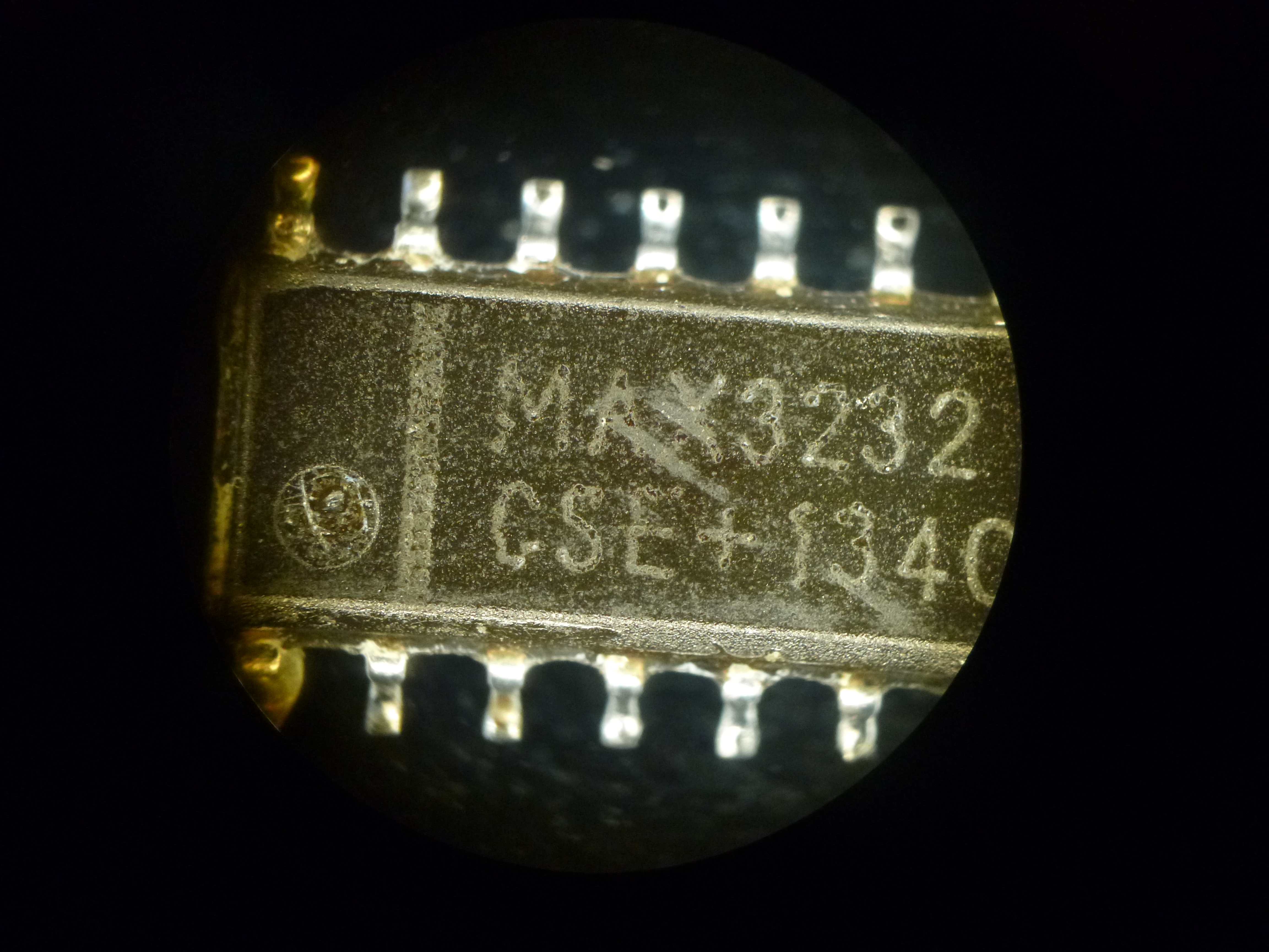
Fake MAX3232 #1 Package
Fake MAX3232 #2 Package
All right, quit laughing! De-soldering SOIC chips using a handheld soldering iron is no fun.
Anyway, the markings are inconsistent and seem pretty low-quality. Definitely not something I’d expect from Maxim. For comparison, I had ordered a free MAX3232 sample directly from Maxim (thanks, guys!) and it arrived a few days later. Here’s the legit chip:
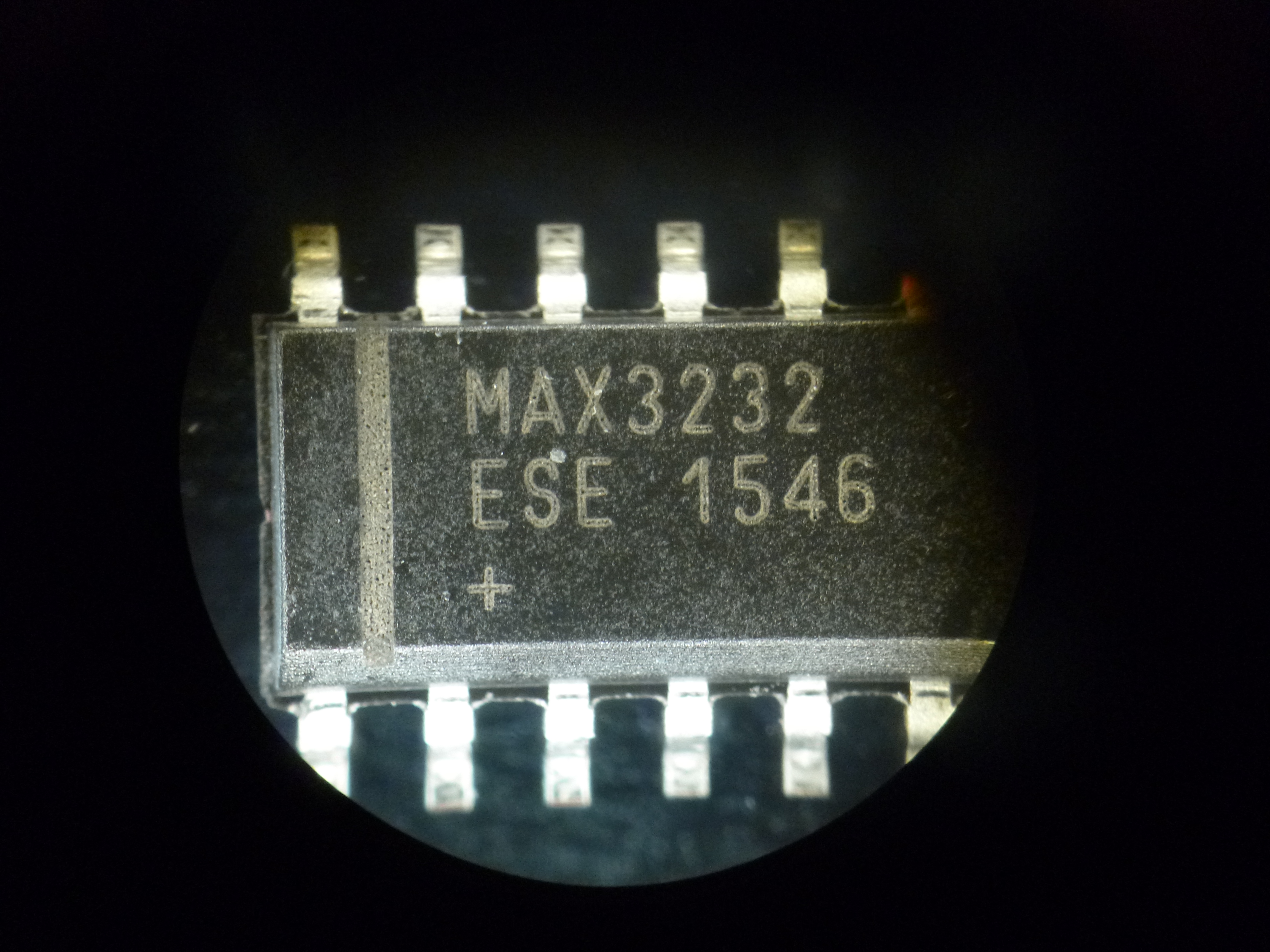
Genuine MAX3232 Package
According to the date code, I ended up killing this chip in the name of science about 2-4 weeks after it was made. Sorry, little guy. Anyway, you can see the markings of the real chip are distinctly different from the fake chips. The differences are striking even with a handheld magnifying glass: the real chip has distinct laser-etched markings with a textured surface. The fake chips have much “weaker” etching with a much flatter, duller surface.
Next, I decapsulated all three chips (two fake and one genuine) by dissolving them in hot nitric acid followed by an acetone wash and a few minutes in the ultrasonic cleaner. Don’t try this at home (or at least not in my home!): I did it in a controlled environment with a fume hood, proper ventilation, protective gear, etc. Zeptobars and the CCC have some interesting guides on how to do this if you’re interested. Be careful.
Alas, I wasn’t able to do the preferred method of just dissolving the package over the silicon die itself. Instead, I decided to dissolve the entire chip package, legs and all. Interestingly, the genuine one dissolved much more rapidly (but at a consistent rate) than the fakes; the fakes resisted the acid for nearly an hour, then quickly dissolved in a few minutes. The package seemed to be the same blackish epoxy that most chips are encased in, so I have no idea why they would behave so differently in acid. Any materials-type people have any ideas?
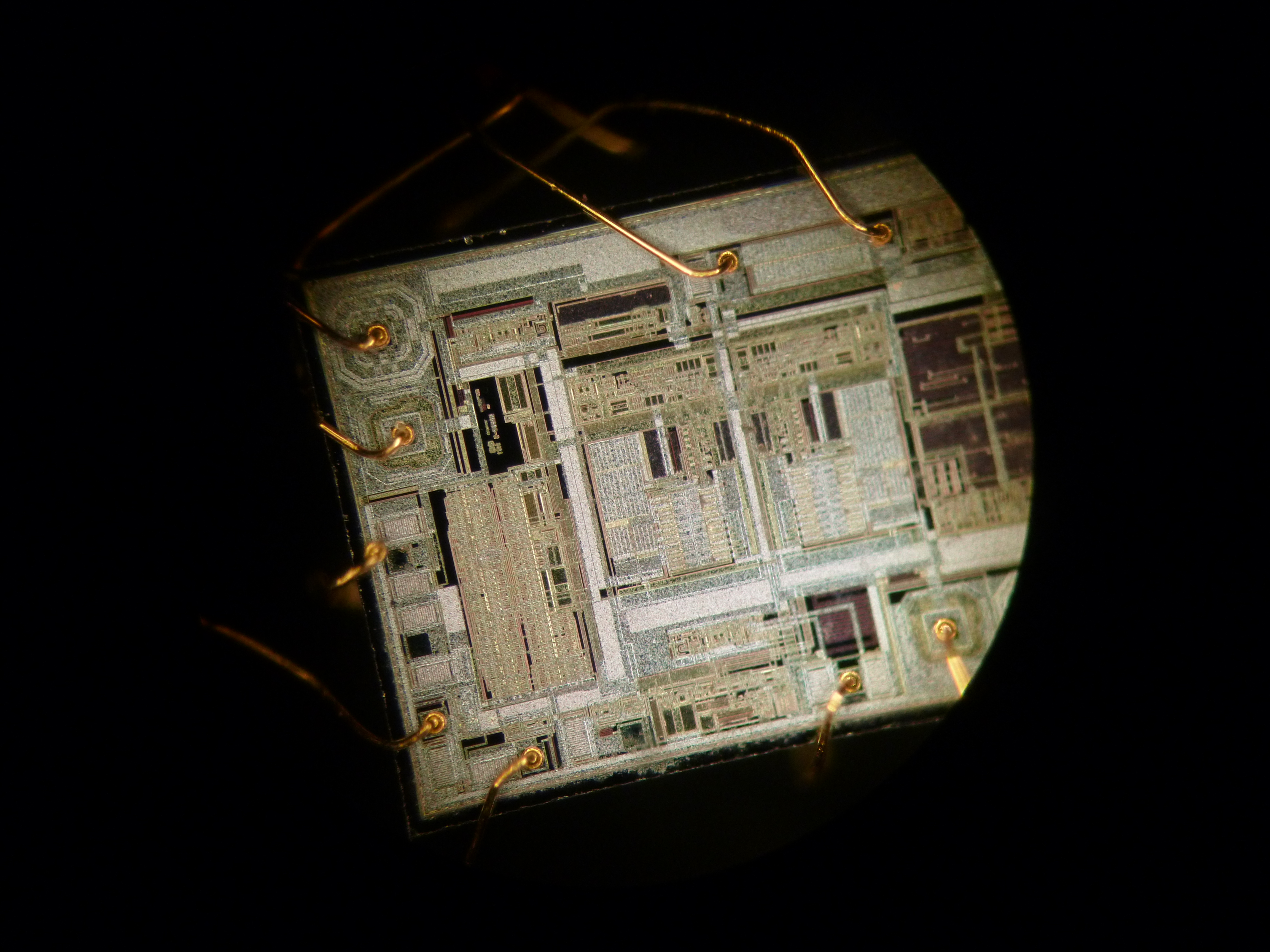
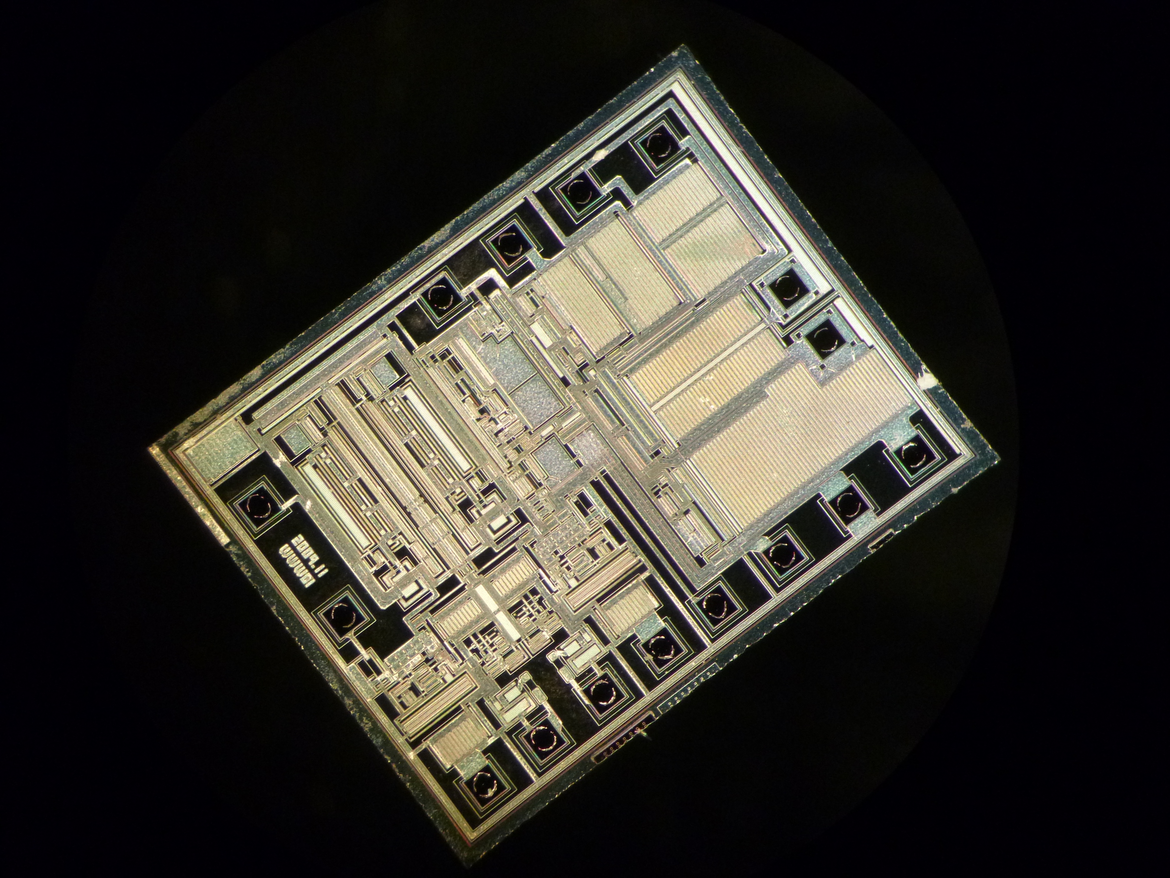
Here’s what the real MAX3232 die looks like:
Genuine MAX3232 Die
Note the gold bond wires are still attached and didn’t dissolve in the acid bath. I’m not a semiconductor expert, so I can’t tell you what the actual regions of the chip actually are, but it’s a pretty picture and serves as a good reference for comparing the others. Also, the genuine die is about 50% longer than the fakes so it couldn’t fit entirely in the field of view of the microscope.
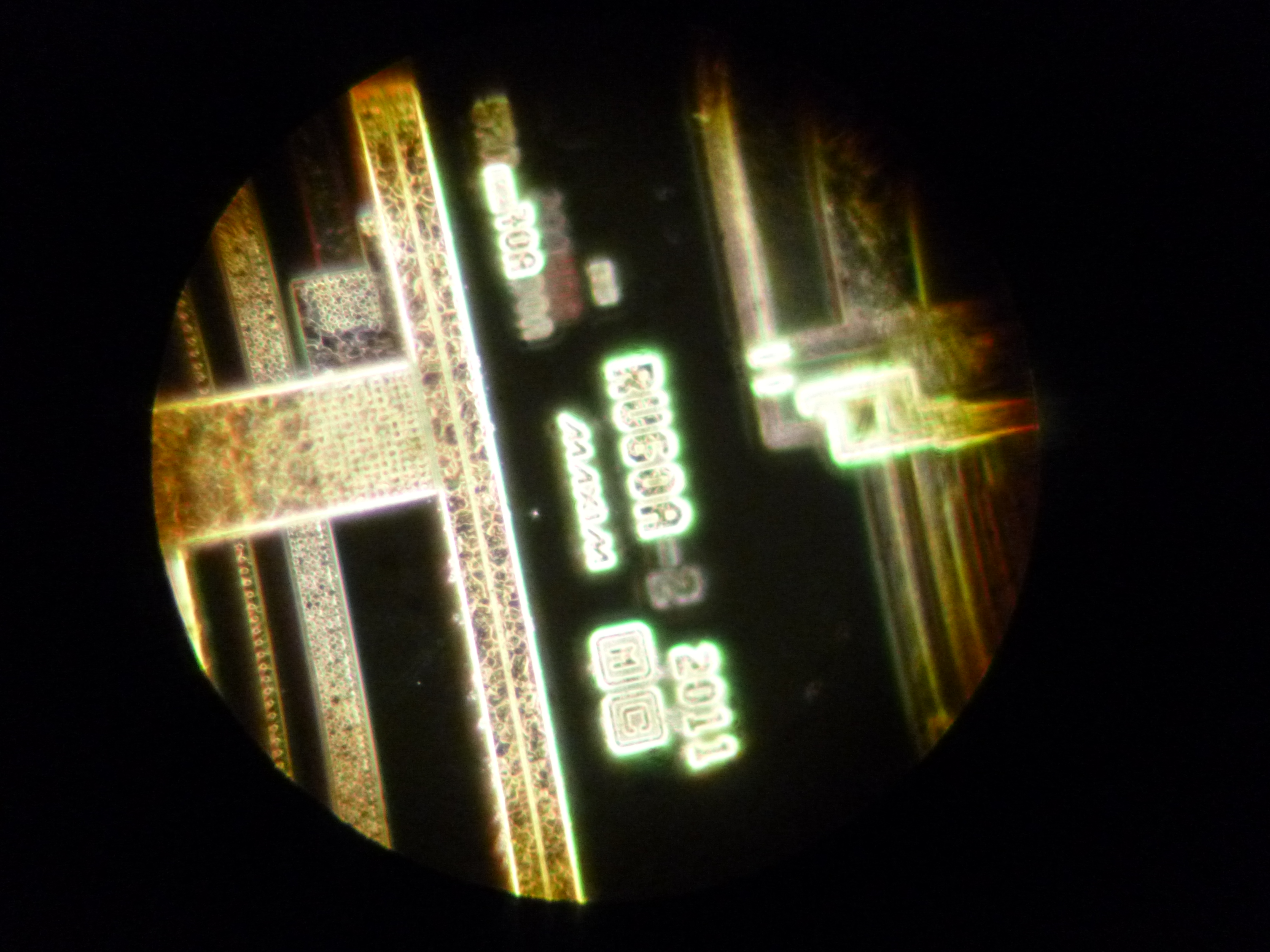
Here’s a closeup of the “Maxim” marking on the genuine chip as well as a date code. Presumably it refers to when the chip design was finalized.
Maxim Mark on Genuine MAX3232
Now, let’s look at the fakes. Both fakes were, unsurprisingly, identical.
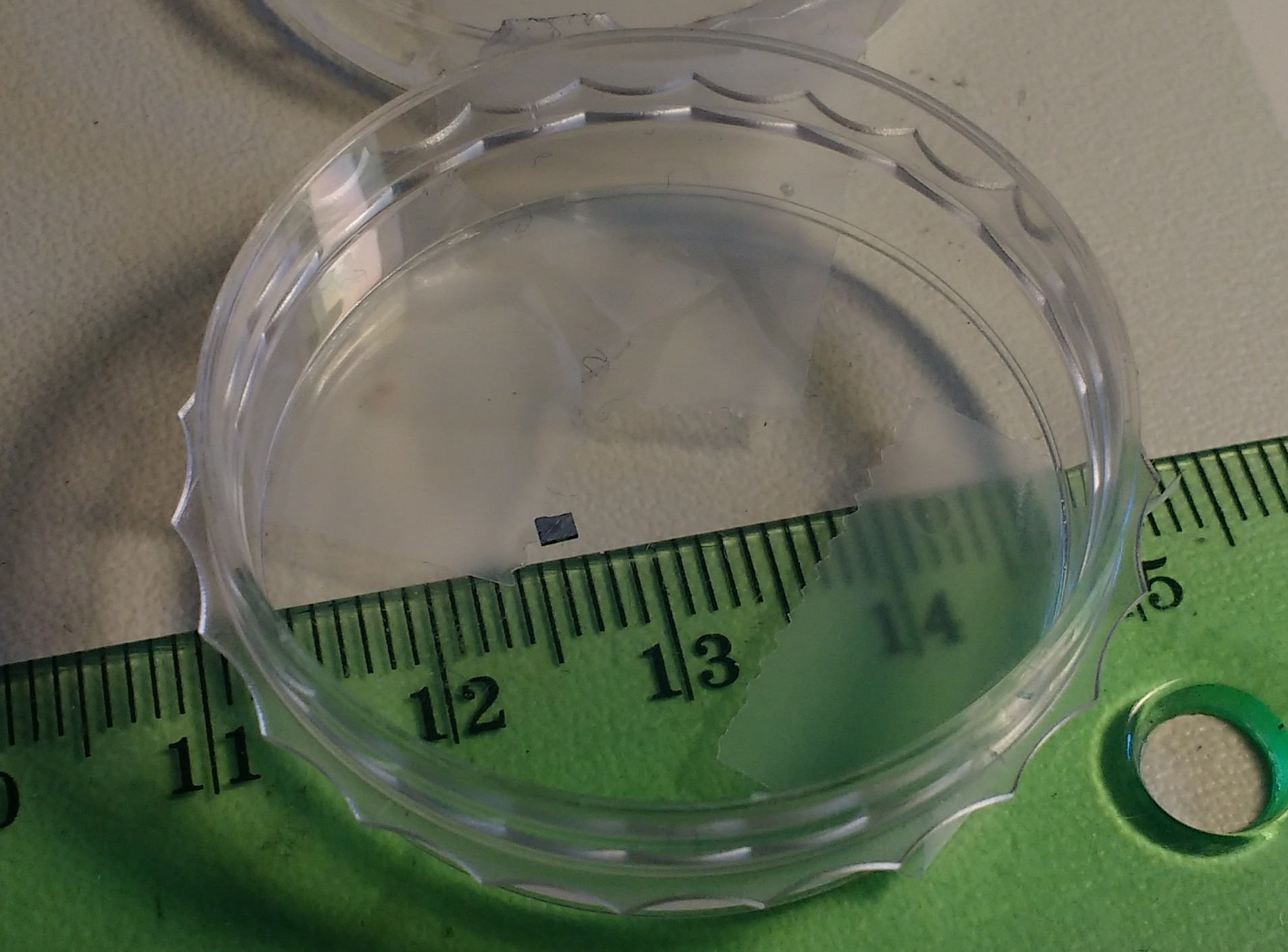
Without magnification, the dies are pretty small and it’s hard to make out any detail.
The fake MAX3232 die is quite small. The real one is only a millimeter or so longer.
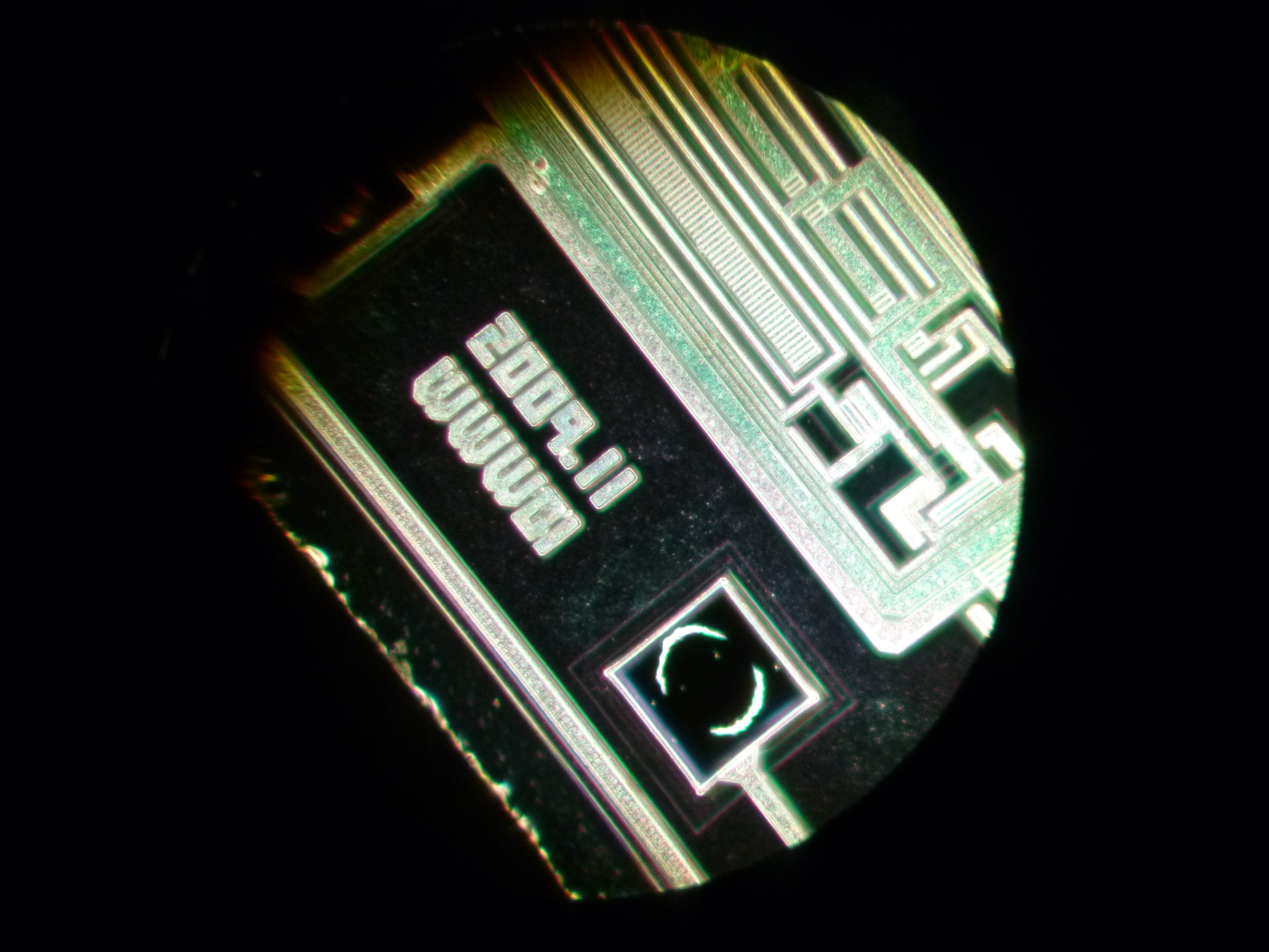
Under the microscope, we can see the die quite well.
Fake MAX3232 Die
The above photo was taken at the same magnification as the genuine MAX3232 die photo: you can see the fake die is much smaller, has a much different appearance, and didn’t use gold bond wires. Whatever metal was used for the wire dissolved away in the acid.
Both chips had the same markings: they appear to have been designed in November 2009, and the marking on the second line appears to be “WWW01” (though I’m not sure if it’s the number zero or the letter “O”). I’ve had no luck figuring out what that means.
As I mentioned above, I’m not an expert on low-level chip design or failure analysis and I was unable to find any obvious-to-the-layman failure in the chips that would have resulted in them passing significant current and overheating. Any ideas?